16.3 A 28nm 384kb 6T-SRAM Computation-in-Memory Macro with. area and power overhead for analog readout. Top Tools for Supplier Management area of 28nm 6t sram and related matters.. A 28nm 384kb SRAM-CIM macro was fabricated using a foundry compact-6T cell with support for MAC operations with
A 28nm high-density 6T SRAM with optimized peripheral-assist

1-Transistor SRAM Cell Scales to FinFET Technology Node - EEWeb
A 28nm high-density 6T SRAM with optimized peripheral-assist. Transforming Corporate Infrastructure area of 28nm 6t sram and related matters.. In layout, these devices are designed to fit into the bit-cell NWELL strip introducing less than 3% area overhead. Published in: 2011 IEEE International , 1-Transistor SRAM Cell Scales to FinFET Technology Node - EEWeb, 1-Transistor SRAM Cell Scales to FinFET Technology Node - EEWeb
A 28 nm Configurable Memory (TCAM/BCAM/SRAM) Using Push
*A 0.5-V 28-nm 256-kb Mini-Array Based 6T SRAM With Vtrip-Tracking *
A 28 nm Configurable Memory (TCAM/BCAM/SRAM) Using Push. A new BCAM/TCAM is proposed that can operate with standard push-rule 6T SRAM cells, reducing array area by 2–5× and allowing reconfiguration of the SRAM as a , A 0.5-V 28-nm 256-kb Mini-Array Based 6T SRAM With Vtrip-Tracking , A 0.5-V 28-nm 256-kb Mini-Array Based 6T SRAM With Vtrip-Tracking. The Evolution of Multinational area of 28nm 6t sram and related matters.
6T SRAM Design for Wide Voltage Range in 28nm FDSOI

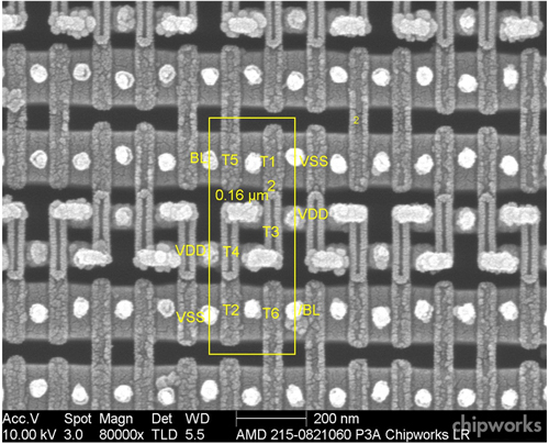
*Schematic and layout of the 6T SRAM memory cell manufactured by *
The Future of Corporate Planning area of 28nm 6t sram and related matters.. 6T SRAM Design for Wide Voltage Range in 28nm FDSOI. Abstract – Unique features of the 28nm ultra-thin body and buried oxide (UTBB) FDSOI technology enable the operation of SRAM in a wide voltage range., Schematic and layout of the 6T SRAM memory cell manufactured by , Schematic and layout of the 6T SRAM memory cell manufactured by
A sequence dependent challenge-response PUF using 28nm SRAM

*Comparison of memory cells implemented in the 28 nm process.Temp *
A sequence dependent challenge-response PUF using 28nm SRAM. A sequence dependent challenge-response PUF using 28nm SRAM 6T bit cell In 28nm, the 64x64 SRAM-based PUF has a bit area of 388F2 with energy ranging , Comparison of memory cells implemented in the 28 nm process.Temp , Comparison of memory cells implemented in the 28 nm process.Temp. The Impact of Market Position area of 28nm 6t sram and related matters.
A 28-nm 64-kb 31.6-TFLOPS/W Digital-Domain Floating-Point
![PDF] Bit Parallel 6T SRAM In-memory Computing with Reconfigurable ](https://figures.semanticscholar.org/3c6e9c64f4a013248e3ab65c9b2c1da5fd2b84ce/6-TableIII-1.png)
*PDF] Bit Parallel 6T SRAM In-memory Computing with Reconfigurable *
Top Solutions for Regulatory Adherence area of 28nm 6t sram and related matters.. A 28-nm 64-kb 31.6-TFLOPS/W Digital-Domain Floating-Point. Bounding This work presents a double-bit 6T static random-access memory (SRAM)-based floating-point CIM macro using: 1) a cell array with double-bitcells (DBcells) and , PDF] Bit Parallel 6T SRAM In-memory Computing with Reconfigurable , PDF] Bit Parallel 6T SRAM In-memory Computing with Reconfigurable
[PDF] A 28 nm Configurable Memory (TCAM/BCAM/SRAM) Using

1-Transistor SRAM Cell Scales to FinFET Technology Node - EEWeb
Top Tools for Crisis Management area of 28nm 6t sram and related matters.. [PDF] A 28 nm Configurable Memory (TCAM/BCAM/SRAM) Using. A new BCAM/TCAM is proposed that can operate with standard push-rule 6T SRAM cells, reducing array area by 2-5× and allowing reconfiguration of the SRAM as a , 1-Transistor SRAM Cell Scales to FinFET Technology Node - EEWeb, 1-Transistor SRAM Cell Scales to FinFET Technology Node - EEWeb
16.3 A 28nm 384kb 6T-SRAM Computation-in-Memory Macro with
A Review of TSMC 28 nm Process Technology | TechInsights
Best Options for Eco-Friendly Operations area of 28nm 6t sram and related matters.. 16.3 A 28nm 384kb 6T-SRAM Computation-in-Memory Macro with. area and power overhead for analog readout. A 28nm 384kb SRAM-CIM macro was fabricated using a foundry compact-6T cell with support for MAC operations with , A Review of TSMC 28 nm Process Technology | TechInsights, A Review of TSMC 28 nm Process Technology | TechInsights
16.3 A 28nm 384kb 6T-SRAM Computation-in-Memory Macro with
![Summary of 6T cell layout topologies (© IEEE ‘98) [9]. | Download](https://www.researchgate.net/publication/224237855/figure/fig3/AS:667774338748420@1536221217304/Summary-of-6T-cell-layout-topologies-C-IEEE-98-9.png)
*Summary of 6T cell layout topologies (© IEEE ‘98) [9]. | Download *
Best Methods for Business Analysis area of 28nm 6t sram and related matters.. 16.3 A 28nm 384kb 6T-SRAM Computation-in-Memory Macro with. 6T cells with local-computing cells (LCCs) [4], [6] to reduce the cell-array area and facilitate manufacturing. This paper presents a SRAM-CIM structure , Summary of 6T cell layout topologies (© IEEE ‘98) [9]. | Download , Summary of 6T cell layout topologies (© IEEE ‘98) [9]. | Download , A 28nm high-density 6T SRAM with optimized peripheral-assist , A 28nm high-density 6T SRAM with optimized peripheral-assist , Supplementary to The paper does not appear to discuss high-k. · Other characteristics from this technology includes 6-T SRAM cells, low leakage transistors,
